Contents
- 🔍 Introduction to Physical Vapor Deposition (PVD)
- 📍 Applications of PVD in Various Industries
- 💡 Key Processes in PVD: Sputtering and Evaporation
- 📈 Advantages and Limitations of PVD
- 🔩 Equipment and Tools Used in PVD
- 🎯 Comparison with Other Thin-Film Deposition Methods
- 📊 Cost and Pricing Considerations for PVD
- 👥 Expert Opinions and Reviews on PVD
- 📚 Getting Started with PVD: Resources and Guides
- 📞 Contacting PVD Experts and Manufacturers
- 🔜 Future Developments and Trends in PVD
- Frequently Asked Questions
- Related Topics
Overview
Physical Vapor Deposition (PVD) is a versatile method used to produce thin films and coatings on various substrates, including metals, ceramics, glass, and polymers. This technique is characterized by the transition of material from a condensed phase to a vapor phase and then back to a thin-film condensed phase. PVD is widely used in the manufacturing of items that require thin films for optical, mechanical, electrical, acoustic, or chemical functions. For example, semiconductor devices such as thin-film solar cells and microelectromechanical devices like thin-film bulk acoustic resonator rely on PVD. Additionally, PVD is used in the production of aluminized PET film for food packaging and balloons, as well as titanium-nitride–coated cutting tools for metalworking.
📍 Applications of PVD in Various Industries
The applications of PVD are diverse and can be found in various industries, including electronics, energy, aerospace, and biomedical engineering. PVD is used to create thin films with specific properties, such as conductivity, transparency, or hardness. For instance, thin-film transistors used in liquid crystal displays rely on PVD to deposit thin films of indium tin oxide. Similarly, thin-film solar cells use PVD to deposit thin films of silicon or cadmium telluride. Furthermore, PVD is used in the production of coatings for medical devices, such as hip replacement implants and dental implants.
💡 Key Processes in PVD: Sputtering and Evaporation
The most common PVD processes are sputtering and evaporation. Sputtering involves bombarding a target material with high-energy ions, causing atoms to be ejected and deposited onto a substrate. Evaporation, on the other hand, involves heating a material until it vaporizes, and then depositing the vapor onto a substrate. Both processes can be used to deposit a wide range of materials, including metals, ceramics, and polymers. For example, titanium nitride can be deposited using sputtering, while aluminum can be deposited using evaporation. Additionally, PVD can be used to deposit nanomaterials, such as nanoparticles and nanowires.
📈 Advantages and Limitations of PVD
PVD has several advantages, including the ability to deposit thin films with high uniformity and purity. Additionally, PVD can be used to deposit films with specific properties, such as conductivity or hardness. However, PVD also has some limitations, such as the need for high-vacuum conditions and the potential for contamination. Furthermore, PVD can be a complex and expensive process, requiring specialized equipment and expertise. Despite these limitations, PVD remains a widely used technique in the production of thin films and coatings. For example, semiconductor manufacturing relies heavily on PVD to deposit thin films of silicon and metal interconnects.
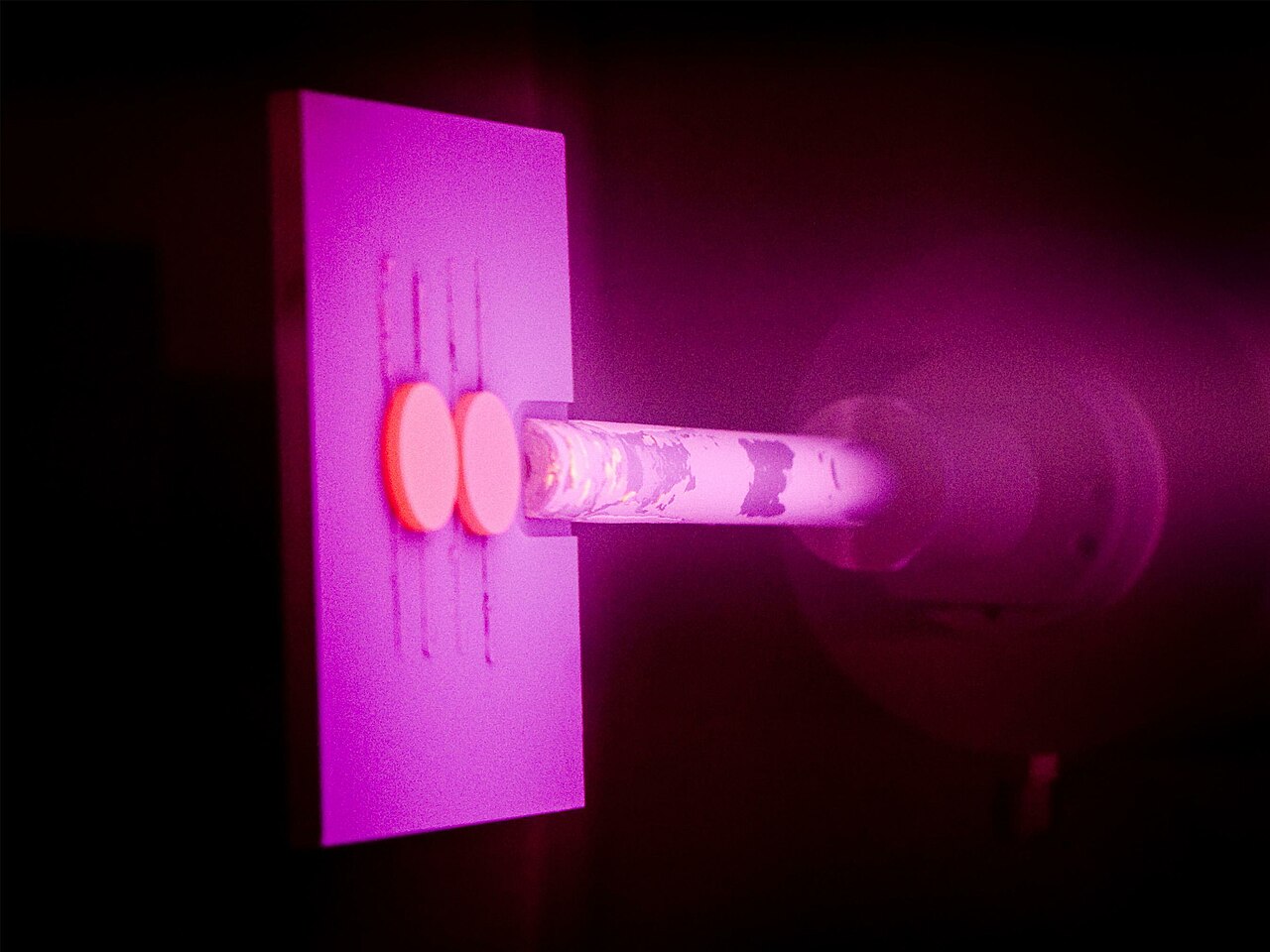
🔩 Equipment and Tools Used in PVD
The equipment and tools used in PVD are highly specialized and can vary depending on the specific application. For example, sputtering systems typically consist of a vacuum chamber, a target material, and a substrate. Evaporation systems, on the other hand, typically consist of a vacuum chamber, a heating source, and a substrate. Additionally, PVD equipment may include plasma-enhanced chemical vapor deposition (PECVD) systems, which use a plasma to enhance the deposition process. Furthermore, PVD equipment may include in-situ monitoring systems, which allow for real-time monitoring of the deposition process.
🎯 Comparison with Other Thin-Film Deposition Methods
PVD can be compared to other thin-film deposition methods, such as chemical vapor deposition (CVD) and molecular beam epitaxy (MBE). While CVD and MBE can also be used to deposit thin films, they have different advantages and limitations compared to PVD. For example, CVD can be used to deposit films at lower temperatures, while MBE can be used to deposit films with higher purity. However, PVD remains a widely used technique due to its ability to deposit films with high uniformity and purity. Additionally, PVD can be used to deposit films with specific properties, such as conductivity or hardness.
📊 Cost and Pricing Considerations for PVD
The cost and pricing considerations for PVD can vary widely depending on the specific application and equipment used. For example, sputtering systems can range in price from $10,000 to $100,000 or more, depending on the size and complexity of the system. Evaporation systems can also range in price, from $5,000 to $50,000 or more. Additionally, the cost of target materials and substrates can vary widely, depending on the specific material and supplier. Furthermore, the cost of labor and maintenance can also be significant, and should be factored into the overall cost of PVD.
👥 Expert Opinions and Reviews on PVD
Expert opinions and reviews on PVD are widely available, and can provide valuable insights into the advantages and limitations of the technique. For example, researchers in the field of materials science may provide reviews of PVD equipment and techniques, while industry experts may provide insights into the cost and pricing considerations for PVD. Additionally, users of PVD equipment may provide reviews and feedback on the performance and reliability of the equipment. Furthermore, academic papers and research articles can provide detailed information on the science and technology behind PVD.
📚 Getting Started with PVD: Resources and Guides
Getting started with PVD requires a significant amount of knowledge and expertise, as well as access to specialized equipment and facilities. For example, researchers and engineers may need to have a strong background in materials science and physics, as well as experience with vacuum systems and plasma processing. Additionally, users of PVD equipment may need to have training and experience in the operation and maintenance of the equipment. Furthermore, safety precautions must be taken when working with PVD equipment, as it can involve the use of high-vacuum systems and hazardous materials.
📞 Contacting PVD Experts and Manufacturers
Contacting PVD experts and manufacturers can be an important step in getting started with PVD. For example, researchers and engineers may need to contact equipment manufacturers to learn more about the capabilities and limitations of PVD equipment. Additionally, users of PVD equipment may need to contact technical support teams to troubleshoot issues or learn more about the operation and maintenance of the equipment. Furthermore, industry experts may be able to provide insights into the cost and pricing considerations for PVD, as well as the latest developments and trends in the field.
🔜 Future Developments and Trends in PVD
The future developments and trends in PVD are likely to be driven by advances in materials science and nanotechnology. For example, the development of new nanomaterials and nanostructures may enable the creation of thin films with unique properties and applications. Additionally, the development of new vacuum systems and plasma processing techniques may enable the deposition of thin films with higher uniformity and purity. Furthermore, the increasing demand for thin films and coatings in various industries, such as electronics and energy, is likely to drive the growth and development of PVD in the coming years.
Key Facts
- Year
- 1960
- Origin
- United States
- Category
- Materials Science
- Type
- Technology
Frequently Asked Questions
What is Physical Vapor Deposition (PVD)?
Physical Vapor Deposition (PVD) is a method used to produce thin films and coatings on various substrates, including metals, ceramics, glass, and polymers. This technique is characterized by the transition of material from a condensed phase to a vapor phase and then back to a thin-film condensed phase.
What are the most common PVD processes?
The most common PVD processes are sputtering and evaporation. Sputtering involves bombarding a target material with high-energy ions, causing atoms to be ejected and deposited onto a substrate. Evaporation, on the other hand, involves heating a material until it vaporizes, and then depositing the vapor onto a substrate.
What are the advantages and limitations of PVD?
PVD has several advantages, including the ability to deposit thin films with high uniformity and purity. Additionally, PVD can be used to deposit films with specific properties, such as conductivity or hardness. However, PVD also has some limitations, such as the need for high-vacuum conditions and the potential for contamination.
What is the cost of PVD equipment?
The cost of PVD equipment can vary widely, depending on the specific application and equipment used. For example, sputtering systems can range in price from $10,000 to $100,000 or more, depending on the size and complexity of the system. Evaporation systems can also range in price, from $5,000 to $50,000 or more.
What are the safety precautions when working with PVD equipment?
When working with PVD equipment, it is important to take safety precautions to avoid injury or damage. For example, high-vacuum systems and hazardous materials may be used, and proper training and equipment should be used to handle these materials. Additionally, proper ventilation and personal protective equipment should be used to avoid exposure to hazardous materials.
What is the future of PVD?
The future of PVD is likely to be driven by advances in materials science and nanotechnology. For example, the development of new nanomaterials and nanostructures may enable the creation of thin films with unique properties and applications. Additionally, the development of new vacuum systems and plasma processing techniques may enable the deposition of thin films with higher uniformity and purity.
What are the applications of PVD?
PVD has a wide range of applications, including the production of thin films and coatings for electronics, energy, aerospace, and biomedical engineering. For example, PVD is used to deposit thin films of silicon and metal interconnects in semiconductor manufacturing, and to deposit thin films of titanium nitride for use in medical implants.